As I am working to improve my PCB design capabilities, I will update this list as a sort of "quality checklist." If you have suggestions to add to this list, drop me a note!
My primary design tool at this point is EasyEDA Pro, and my primary PCB producer is JLCPCB.
General Checklist
Four-layer PCB for most projects. If using six layers, stackup of signal-ground-power-signal-ground-signal.
Inner VCC plane
Inner GND plane
Top layer with copper fill (VCC?). This is required by JLCPCB if using track spacing of less than 0.15mm.
Bottom layer with copper fill (GND?). This is required by JLCPCB if using track spacing of less than 0.15mm.
1oz copper
Via drill hole (inner diameter) of 0.3mm. Via outer diameter of 0.4mm. Smaller values will significantly increase the PCB cost.
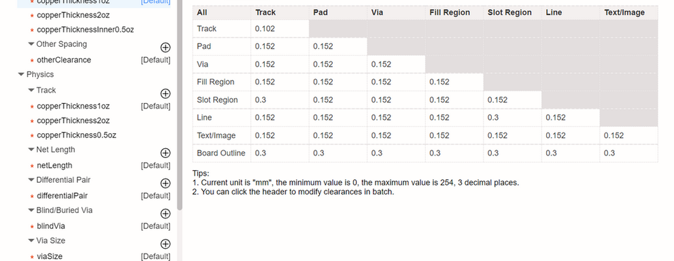
Track width of 0.152mm. Wider for VCC/GND, as possible.
Track spacing of 0.152mm
Pad spacing of 0.152mm
Via spacing of 0.152mm
Board outline spacing of 0.3mm
Standoffs
Test points
ENIG for BGA PCBs
Via Covering: Epoxy Filled & Capped for BGA PCBs when using via-in-pad
...
I have some additional thoughts captured here: 486DLC >>> 486DX PCB Design Updates (rehsdonline.com).
Lattice CT256 BGA
As I make progress on routing a 256-pin iCE40 FPGA, I'll post my config here.
Part: ICE40HX8K-CT256
Balls: 256
Package: caBGA
Size: 16mm x 16mm
Pitch: 0.8 mm
I/O: 206
General lnformation
Six-layer PCB
Below are Lattice recommendations for this BGA, along with JLCPCB capabilities. Bolded values are what I am using.
Specification | Lattice Sample Spec | JLCPCB Capability (as of Feb 2024) |
BGA Solder Pad Size | 0.2000 mm | 0.2500 mm Via-in-pad recommended: 0.4000 mm System device default: 0.3600 mm |
BGA Pad Solder Mask | 0.3400 mm | ? |
BGA Via Size (Drill) | 0.1270 mm | 0.2000 mm |
BGA Via Size (Pad) | 0.2540 mm | 0.3000 mm |
Trace Width | 0.1270 mm | 0.0900 mm |
Trace Spacing | 0.0889 mm | 0.0900 mm |
BGA Pad Spacing | 0.1270 mm | |
Trace to BGA Pad Spacing | 0.1270 mm | |
Via Copper to BGA Pad Spacing | 0.1270 mm | |
innerPlane Network Spacing copperRegion Network Spacing (pad to pour) | 0.2000 mm | |
No support for buried or blind vias. |
General Steps
Create a new project in EasyEDA Pro. Configure stack up with six layers, four of which should be signal and two planes. Example from bottom up: signal, signal, POWER, GND, signal, signal. See TN1074.
Configure design rules according to the table above.
Start with the CE40HX8K-CT256 FPGA device from the EasyEDA Pro System library. The default pad is 0.3600 mm.
Apply fanout setting, using Via in Pad.
Delete the pads in the outer three rows/columns. The Filter tab is handy for quickly filtering selectable objects to just the vias. Then, drag around vias to be deleted and delete.
Place capacitors and connect with vias.
Add copper fills on inner POWER plane.
Route all signals.
Check for DRC errors and clean up appropriately.
Lattice Sample Recommendation


EasyEDA Pro Defaults (JLCPBC multi-layer)
EasyEDA Pro - Routed caBGA for JLCPCB
Changes from EasyEDA Pro Defaults
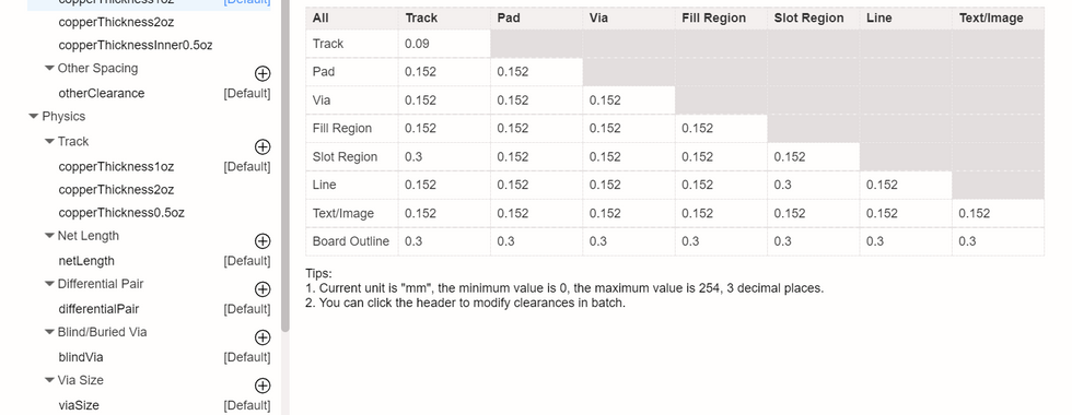
Track width to 0.1mm
Track spacing to 0.1mm
Via drill size to 0.2mm
Via diameter to 0.3mm
InnerPlane Network Setting (pad to pour) to 0.2mm
For copper fills, set Optimization to No
To consider:
Increase BGA pad to 0.4mm (from 0.36mm)
Increase via diameter to 0.35mm (from 0.30mm)
...


Commentaires