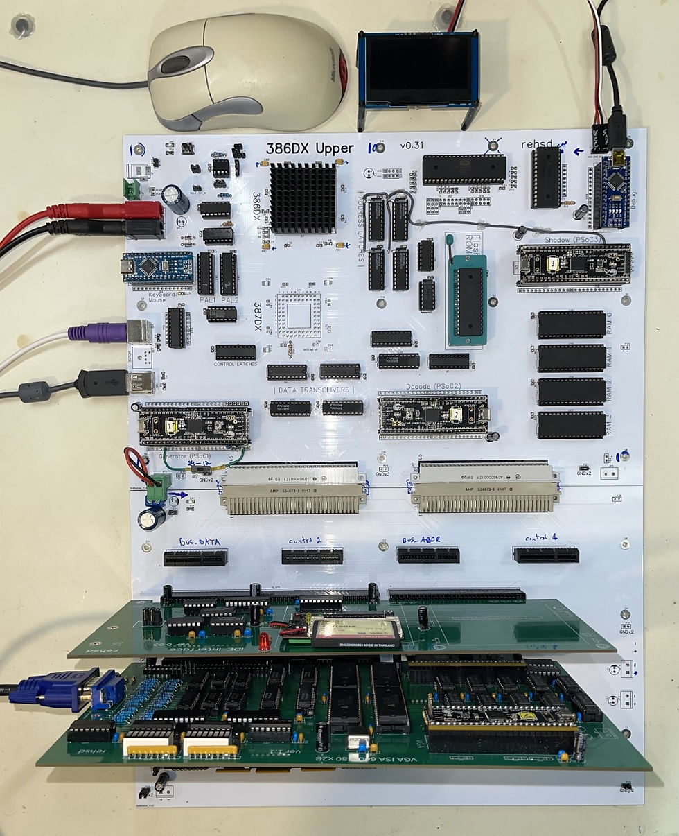
As I have gotten my 386 DX upper and lower motherboard PCBs working -- at least to the point of validating much of the design -- I am now considering what the next revision of the motherboard might look like. My primary goal is to improve signal quality and general PCB design. I am hoping to learn more about best practices in PCB design and apply some of those concepts.
In this post, I will track some of my thoughts, suggestions from others, and what my general plan will be. I will also share updates on the PCB design as I update the schematic and PCB. I will continue to post updates here, so check back!
I'm considering make a pivot to the 486DX at this stage. This will remove the 387DX from the PCB. That, along with the PSoC consolidation frees up space and simplifies routing. However, the 486DX requires byte swapping logic and associated transceivers.
Objectives / Constraints
Here are the key objectives and constraints for me as I work on an updated PCB.
486DX focused.
ATX form factor, especially in regards to size and mounting.
Four or six layer PCB. My current PCB is a two-layer PCB. The jump to four-layer is costly, but the additional jump to six-layer in relatively small. Beyond six-layer, cost jumps more rapidly. I'm targeting a six-layer PCB as the best value option for me that is greater than two-layer.
More surface mount than I have typically used.
Leave room in the design for future expansion or current unknowns.
Debug-friendly PCB (e.g., easily-access test points). I do not plan to include debug headers for my Agilent logic analyzers. While I would love to include these, they take up precious space and complicate routing.
Leverage components that are readily available and inexpensive.
...
Current Plan
At this point, I am targeting a single 486DX motherboard.
2MB of SRAM for memory.
Single PSoC for PLD support for control signal generation, decode logic, and shadowing ROM to RAM.
No support for DRAM, caching, or DMA.
Onboard SPI support.
I/O expansion slots support 32-bit addressing and data.
Series termination (inline resistor) for address and control lines.
Thevenin's Equivalent termination (pull-up + pull-down) on data lines.
Experimenting with PCB trace width: 0.2mm; via diameter: 0.61mm; via drill diameter: 0.305mm.
Suggestions
Here are suggestions I have received from the community. I very much appreciate these. Keep them coming!
Use as much surface-mount as possible. They are smaller and do not require mounting holes. Along with this, place components on both sides of the board.
Instead of socketed PSoC and Arduino Nano devices, place these directly on the PCB.
Move the logic handled by discrete ICs into the PSoCs.
Possible six-layer stackups: signal-ground-power-signal-ground-signal, or signal-ground-signal-signal-power/ground-signal.
Place all caps around PSoC chips on the bottom side of the board.
LCPCB 6+ layer boards come with via-in-pad technology for free, so you can place a bunch of vias on a thermal pad of QFNs - they will be covered and plated over.
Extend QFN pads farther outside so that they can be touched up with an iron if needed.
...
PCB Design Considerations
As I am researching PCB design and getting tips from others, I will capture considerations below. References in parentheses are to numbered items in the References section, followed by the page number. The following considerations are in no particular order at this point. If you have suggestions for additions, please drop me a note!
Outer-layer PCB traces are always faster than inner traces. (1, pg. 7)
Given two logic families with identical maximum propagation delays, the family with the slowest output switching time will be cheaper and easier to use. (1, pg. 66)
Eliminate reflections by reducing end termination, reducing series termination, or making sure the line is short. (1, pg. 167)
Capacitive loads degrade the rise time of passing signals and reflect pulses back upstream. Uniformly distributed capacitive loads reduce a transmission line's effective impedance and slow it down. A printed circuit trace makes an effective small delay line. (1, pg. 177)
If using a two-layer PCB, use the power and ground grid system. (1, pg. 199)
The rise time of an end-terminated circuit, when capacitively loaded, is half that of a series-terminated line driving the same load. Most TTL or CMOS logic gates can't source enough current to drive end terminators. (1, pg. 231)
Source terminators have a slower rise time and usually smaller residual reflections than end terminators. (1, pg. 235)
DIP isolated resistor networks have lower mutual inductance compared to SIPs. (1, pg. 247)
An array of bypass capacitors is more effective than a single bypass capacitor. (1, pg. 260)
For power, the best way to get low inductance is to parallel a lot of small capacitors (bypass). (1, pg. 276)
Spread grounds across connectors to reduce crosstalk. (1, pg. 300)
Clock skew has as much an impact on overall operating speed as any other propagation delay.
Vias, when used in traces, are capacitive, not inductive. (2, pg. 93)
Termination Characteristics. (3, pg. 13)

Autorouters for PCBs do not take any noise reduction actions; therefore, care should be taken in their use. Power and ground routing, as well as signals that impact susceptibility, should be laid out by hand. Any signal with clocked data, such as low address bits in a memory expansion bus, should be next. Only signals with switching rates below 50 kHz can be left safely to the autorouter. (3, pg. 16)
"High speed" is likely 40Mhz or greater. (4, pg. 10)
Keep all high-speed signals of the same group of signals on the same layer to avoid skew. (4, pg. 34)
Signal integrity problems are caused by fast driver edge rates, comparatively long interconnects between driver and receiver pins, and impedance discontinuities or mismatches. (5, pg. 398)
As a general rule, any line with an edge rate faster than about 5 ns on nets running longer than an inch should be considered for termination. (5, pg. 406)
Source termination is useful in point-to-point, unidirectional connections. Far-end terminations is useful in multipoint connections. Distributed termination can be helpful in a plug-in systems with variable configuration. (5, pg. 407)
The Intel i486 Microprocessor Hardware Reference Manual has some nice information on termination.
...
IC Selection
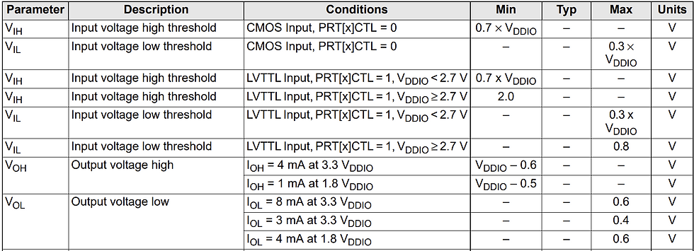
One area I am hoping to dial in better is my selection of IC families. I need to pay attention to timing-related data (e.g., tpd) and voltage levels (e.g., VOH, VIH, VOL, VIL). 7400-series integrated circuits - Wikipedia has basic information about tpd for 7400-series ICs. Data sheets will be helpful. I would like to dig deeper into static timing analysis.
For levels, Texas Instruments has a handy reference at Logic Guide (Rev. AB) (ti.com). To the right are two excerpts, relevant to my build. Again, data sheets will be helpful as I look at levels of all my components. From the table, it seems like my biggest concern will be if I have any TTL drivers with CMOS receivers (that are not TTL compatible).
Miscellaneous notes related to this:
The i486 clock must be TTL, 0.3V to 0.8V for a logic low and 2.0V to VCC plus 0.3V for a logic high.
Cx486DLC VOL of 0.45V max, VOH of 2.4V min, VIL -0.3V to 0.8V, VIH 2.0V to VCC plus 0.3V.
AS6C4008 SRAM is CMOS with TTL-compatible output.

For the PSoCs, VIL 1.5V max, VIH 3.5V min, VOL 0.4V max, VOH, 4.5V min.

For the GALs, VIL 0.8V max, VIH 2.0V min, VOL 0.5V max, VOH, 2.4V min.

More research to do...
As I look at my 7400 series ICs, from what I can tell above, I should be sticking with AHCT, HCT, or ACT. HCT are probably ruled out due to speed. ACT can cause ground bounce. AHCT might be a good option, or possibly F or AS. I am leaning towards F as this stage. Suggestions?
Processors
As I am now looking at a 486DX2 (or DX or DX4), I will ideally find a CPU that is 5V for operating voltage and I/O, has a static core, in a PGA package.
ST486DX2-66GS is 5V, fully static design, PGA.
...
Additional Research Needed
Below is a list of content that is in my queue for review (related to PCB design guidance).
i486 Hardware Reference Manuals
...
Schematic
Here is the latest version of the schematic, which is a work in progress.
References
High-speed Digital Design: A Handbook of Black Magic
Right the First Time: A Practical Handbook on High Speed PCB and System Design
Printed Circuits Handbook, Seventh Edition
...
Additional Resources
PCB Order Checklist
More for my reference than anything, below is a checklist I am building for design review prior to ordering PCBs.
Inner layers set to Signal or Plane. All planes have net set (e.g., VCC copper set to VCC net).
Keep out areas setup for board edges, including lower portions of edge connectors.
Components re-annotated (re-numbered).
Complete, helpful silkscreens.
... (more to come)


Kommentare